Advanced semiconductor packaging technology plays a crucial role in modern electronic devices, enabling higher performance, miniaturization, power efficiency, and cost-effectiveness. Here is an analysis of key aspects and trends in advanced semiconductor packaging technology:
1. Miniaturization and Form Factor:
- System-in-Package (SiP): Integration of multiple components (like processors, memory, sensors) into a single package for compact devices.
- Wafer-Level Packaging (WLP): Packaging chips directly on the wafer level, reducing the overall size of the final product.
2. High-Performance Computing:
- 3D Packaging: Stacking multiple dies vertically to increase performance and reduce interconnect lengths for faster data transfer.
- Heterogeneous Integration: Combining different technologies like CPUs, GPUs, and memory in a single package for improved performance.
- Through-Silicon Via (TSV): Vertical interconnects passing through silicon wafers, enabling high-bandwidth communication between stacked dies.
3. Power Efficiency and Thermal Management:
- Fan-Out Wafer-Level Packaging (FOWLP): Enhancing power efficiency and thermal performance by distributing components across a larger area.
- Embedded Die Packaging: Integrating components directly into the PCB for better thermal dissipation and power management.
4. Connectivity and Data Transfer Speeds:
- Advanced Interconnects: Use of advanced materials like copper, silver, and interposers for higher signal speeds and data transfer rates.
- High-Density Interconnect (HDI): Increasing the number of connections in a smaller area for faster data transfer.
5. Reliability and Durability:
- Underfill and Encapsulation Materials: Enhancing mechanical strength and protecting components from external stress and environmental factors.
- Reliability Testing: Advanced testing methodologies to ensure performance under various conditions and stress factors.
6. Cost-Effectiveness and Volume Production:
- Fan-Out Panel-Level Packaging (FOPLP): Cost-effective approach for large-scale semiconductor packaging using panel-sized substrates.
- Chip-on-Board (COB): Directly mounting unpackaged semiconductor chips onto PCBs for cost savings and increased production efficiency.
7. Emerging Trends and Technologies:
- Fan-Out System-in-Package (FSoP): Integrating high-density components in a single package for advanced applications like 5G, AI, and IoT.
- Chiplets and Modular Designs: Breaking down a system into smaller, individual components (chiplets) for flexibility and scalability in manufacturing and assembly.
- Advanced Materials and Processes: Incorporating new materials like organic substrates, advanced polymers, and improved lithography techniques for enhanced performance.
8. Industry Standards and Collaboration:
- Advanced Packaging Standards (e.g., JEDEC): Ensuring interoperability and compatibility between components and devices.
- Industry Collaboration: Partnerships between semiconductor manufacturers, packaging companies, and research institutions to drive innovation and standardization.
Conclusion:
Advanced semiconductor packaging technology is evolving rapidly to meet the demands of increasingly complex electronic systems. Innovations in packaging play a critical role in enabling next-generation devices with improved performance, efficiency, and reliability. By leveraging diverse packaging techniques and embracing emerging trends, the semiconductor industry aims to push the boundaries of technology and drive forward the development of cutting-edge electronic devices.
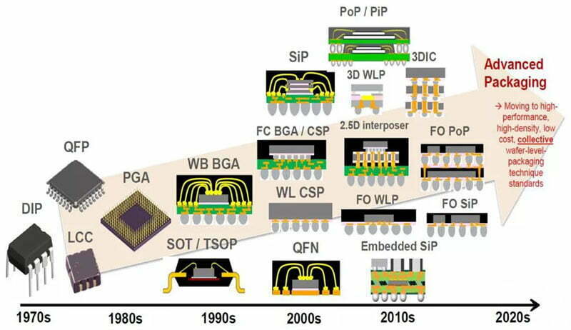
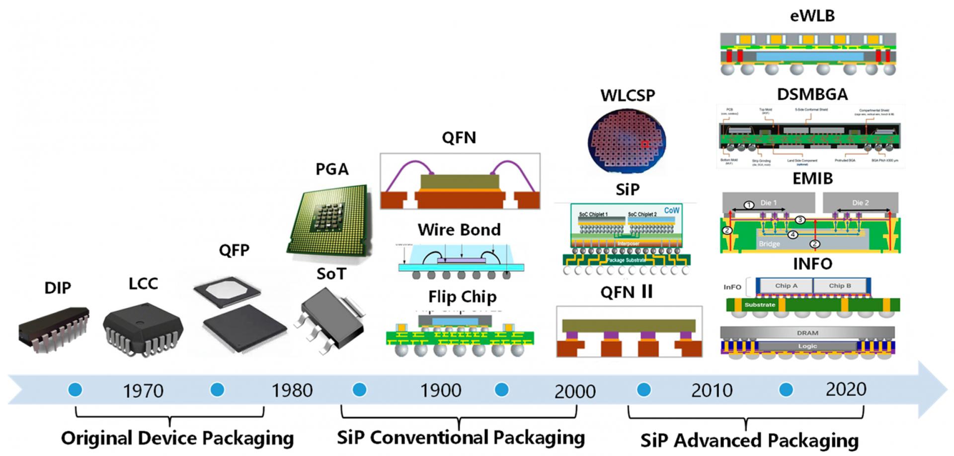
Development of integrated circuits and packaging
The development of integrated circuits (ICs) and packaging has undergone significant transformations over the years, catalyzing advancements in electronics, computing, telecommunications, and various other industries. Here is an overview of the evolution and key developments in integrated circuits and packaging:
Early Development:
- 1950s - Invention of the Integrated Circuit:
- The integrated circuit was invented in the late 1950s by engineers like Jack Kilby and Robert Noyce, leading to the miniaturization of electronic circuits.
- 1960s - Early Chip Development:
- Early ICs were made using small-scale integration (SSI) and medium-scale integration (MSI) techniques, combining a few to several logic gates on a single chip.
Advancements in IC Development:
-
1970s - Large-Scale Integration (LSI):
- The 1970s saw the rise of LSI technology, allowing hundreds to thousands of transistors to be integrated onto a single chip, enabling more complex functionalities.
-
1980s - Very Large-Scale Integration (VLSI):
- VLSI technology emerged in the 1980s, enabling the integration of thousands to millions of transistors on a single chip. This led to the development of microprocessors and memory chips.
-
1990s - System-on-Chip (SoC):
- SoC designs integrated entire systems, combining processors, memory, input/output interfaces, and more on a single chip, enhancing performance and reducing space requirements.
-
2000s-Present - Ultra-Large-Scale Integration (ULSI) and Advanced Packaging:
- ULSI technology pushed the limits of integration, with billions of transistors now being integrated into advanced microprocessors, GPUs, and ASICs.
- Advanced packaging techniques like flip-chip packaging, system-in-package (SiP), and 3D packaging have enabled denser and more efficient designs.
Evolution of Packaging Technologies:
-
Dual In-Line Packages (DIP) and Through-Hole Technology:
- Early ICs were housed in DIP packages, with leads inserted into holes on PCBs for connections.
-
Surface-Mount Technology (SMT):
- SMT replaced through-hole technology, enabling components to be mounted on the surface of PCBs, enhancing assembly efficiency and density.
-
Advanced Packaging Techniques:
- Ball Grid Array (BGA): Solder balls replace leads for better connections and thermal characteristics.
- Chip Scale Packages (CSP): Compact packages directly mounted on the die's footprint for space efficiency.
-
3D Packaging:
- Stacking and interconnecting multiple dies vertically to increase performance, reduce footprint, and enhance data transfer rates.
-
Wafer-Level Packaging (WLP):
- Packaging chips directly at the wafer level to reduce package size, improve thermal performance, and lower costs.
Current Trends and Future Directions:
-
Heterogeneous Integration: Combining different technologies like CPUs, GPUs, and memory in a single package for improved performance and functionality.
-
Advanced Interconnects: Employing new materials and techniques for faster data transfer speeds and reduced power consumption.
-
Multi-Chip Modules (MCM) and Chiplets: Breaking down systems into modular components for scalability and customization.
-
Advanced Materials: Exploring new materials like organic substrates and advanced polymers for enhanced thermal and electrical properties.
The development of integrated circuits and packaging has revolutionized the electronics industry, enabling the creation of increasingly complex and powerful electronic devices. Continued innovation in IC design and packaging techniques is driving the development of next-generation technologies, ushering in an era of more efficient, compact, and high-performance electronic systems.
Semiconductor packaging technology
Semiconductor packaging technology refers to the methods and processes used to protect and connect semiconductor devices like integrated circuits (ICs) to facilitate their use in electronic systems. Packaging is essential for ensuring the functionality, reliability, and performance of semiconductor devices. Here is an overview of semiconductor packaging technology:
Importance of Semiconductor Packaging:
-
Protection: Packaging shields semiconductor devices from environmental factors like moisture, dust, and mechanical stresses.
-
Interconnection: It provides a means to connect the semiconductor device to the external circuitry, enabling data and power transfer.
-
Thermal Management: Packaging helps dissipate heat generated by the semiconductor device during operation, maintaining optimal temperature conditions.
Types of Semiconductor Packaging:
-
Through-Hole Technology (THT): Components are mounted with wire leads inserted into holes on the PCB.
-
Surface-Mount Technology (SMT): Components are mounted directly onto the surface of the PCB for denser and more efficient assembly.
-
Ball Grid Array (BGA): Solder balls under the package provide electrical connections, aiding in thermal dissipation.
-
Quad Flat Packages (QFP), Small Outline Packages (SOP), and Dual In-Line Packages (DIP): Common traditional packaging styles.
-
Chip-Scale Packages (CSP) and Wafer-Level Packaging (WLP): Compact packages that are close to or the same size as the semiconductor die.
Advancements in Semiconductor Packaging Technology:
-
Advanced Interconnect Techniques:
- Flip-Chip Bonding: Directly connects chip pads to substrate to reduce signal propagation delays.
- Wire Bonding: Uses fine wires to connect the chip to the package leads.
-
System-in-Package (SiP): Integration of multiple components into a single package to reduce size and enhance performance.
-
3D Packaging: Stacking multiple dies vertically to boost performance, reduce footprint, and enhance interconnectivity.
-
Fan-Out Wafer-Level Packaging (FOWLP): Distributes components across a larger area to improve power efficiency and thermal performance.
-
Heterogeneous Integration: Combining different technologies (e.g., CPUs and memory) in a single package for enhanced functionality.
-
Advanced Materials: Use of materials with better thermal conductivity and electrical properties to improve performance and reliability.
Emerging Trends and Future Directions:
-
Advanced Thermal Solutions: Innovations to manage heat effectively in high-performance devices.
-
Chiplet Integration: Modularity in packaging to facilitate scaling and customization.
-
Embedded Die Packaging: Integrating components directly into the PCB for enhanced thermal dissipation and miniaturization.
-
Advanced Testing and Inspection Techniques: Ensuring high reliability and quality in complex semiconductor packages.
In conclusion, semiconductor packaging technology plays a pivotal role in the performance and functionality of electronic devices. Advances in packaging techniques are essential for meeting the evolving demands of modern electronics, such as higher performance, miniaturization, and enhanced functionality. Continued innovation in semiconductor packaging technology is essential for driving the development of next-generation electronic devices that power our interconnected world.
advanced packaging technology analysis
Advanced packaging technology plays a critical role in the semiconductor industry, enabling increased functionality, performance, and miniaturization in electronic devices. Here is an in-depth analysis of advanced packaging technology and its impact on the semiconductor industry:
Evolution of Advanced Packaging Technology:
-
Miniaturization and Integration:
- System-in-Package (SiP): Integrating multiple components into a single package to reduce footprint and enhance performance.
- Wafer-Level Packaging (WLP): Packaging chips directly on the wafer level for improved efficiency and miniaturization.
-
High-Performance Computing:
- 3D Packaging: Stacking multiple dies vertically to increase performance and reduce interconnect lengths for faster data transfer.
- Heterogeneous Integration: Combining different technologies (e.g., CPUs, GPUs, memory) for enhanced functionality.
-
Power Efficiency and Thermal Management:
- Fan-Out Wafer-Level Packaging (FOWLP): Enhancing power efficiency and thermal performance by distributing components across a larger area.
- Embedded Die Packaging: Integrating components directly into the PCB for efficient thermal dissipation.
Key Trends and Technologies in Advanced Packaging:
-
Multi-Chip Modules (MCM) and Chiplets:
- Breaking down systems into smaller modules for scalability, customization, and improved yield rates.
-
Advanced Interconnects:
- Through-Silicon Via (TSV): Vertical interconnects enabling high-bandwidth communication in stacked dies.
- High-Density Interconnect (HDI): Increasing the number of connections for faster data transfer.
-
Emerging Packaging Techniques:
- Fan-Out System-in-Package (FSoP): Integrating high-density components in a single package for advanced applications.
- Chip-on-Board (COB): Directly mounting unpackaged chips on PCBs for cost savings and efficiency.
-
Advanced Materials and Processes:
- Organic Substrates and Polymers: Offering improved thermal and electrical properties for enhanced performance.
- Advanced Lithography Techniques: Enabling finer line widths and denser chip designs.
Impact on Industry and Applications:
-
Improved Performance: Advanced packaging technologies enable higher speeds, lower power consumption, and improved signal integrity.
-
Enhanced Functionality: Complex functionalities with a smaller footprint, leading to innovative products in various sectors like IoT, AI, and 5G.
-
Cost-Effectiveness: Enhanced yields, lower fabrication costs, and better efficiency in manufacturing processes.
-
Reliability and Durability: Advanced packaging techniques ensure devices are more robust, reliable, and can withstand harsh environmental conditions.
Future Directions and Challenges:
-
Heterogeneous Integration: Integration of diverse technologies on a single package.
-
5G and IoT Demands: Meeting the demands for faster data processing and connectivity in emerging technologies.
-
Thermal Management: Effective cooling solutions for higher-performance chips in compact packages.
-
Standardization and Compatibility: Ensuring interoperability and compatibility across different technologies and manufacturers.
In conclusion, advanced packaging technology continues to drive innovation in the semiconductor industry, enabling the development of smaller, faster, and more efficient electronic devices. As the demand for higher performance and functionality increases, advanced packaging technologies will play a crucial role in shaping the future of semiconductor devices and their applications across various industries.

Application examples of advanced packaging
Advanced packaging technologies are crucial for enabling high-performance, compact, and power-efficient electronic devices across various industries. Here are some application examples where advanced packaging plays a significant role:
1. Consumer Electronics:
- Smartphones: Advanced packaging techniques like System-on-Chip (SoC) integration, 3D packaging, and wafer-level packaging enable the compact design and high-performance features of smartphones.
- Wearable Devices: Miniaturized components using advanced packaging enable the development of lightweight and feature-rich wearables like smartwatches and fitness trackers.
2. Automotive Industry:
- Advanced Driver Assistance Systems (ADAS): Advanced packaging in automotive electronics ensures reliable and robust components for safety-critical applications like collision avoidance systems and autonomous driving technologies.
- Electric Vehicles (EVs): Efficient power modules and thermal management through advanced packaging contribute to the performance and reliability of EV components like motor controllers and battery management systems.
3. Data Centers and Cloud Computing:
- High-Performance Computing: 3D packaging and advanced interconnects support high-speed data processing in data centers, improving computational efficiency and reducing latency.
- Artificial Intelligence (AI) Accelerators: Advanced packaging technologies enable the integration of GPUs, TPUs, and memory in AI accelerators for faster data processing and machine learning tasks.
4. Internet of Things (IoT):
- Edge Computing Devices: Compact form factors using advanced packaging allow for efficient IoT devices with enhanced computing power and connectivity.
- Sensor Networks: Miniaturized sensor nodes with advanced packaging enable IoT applications in smart homes, industrial automation, and environmental monitoring.
5. Medical Devices:
- Implantable Electronics: Advanced packaging ensures biocompatibility, reliability, and miniaturization in implantable medical devices like pacemakers and neurostimulators.
- Medical Imaging Systems: Advanced packaging techniques support high-resolution imaging systems such as MRI machines and ultrasound devices for accurate diagnostics.
6. Aerospace and Defense:
- Avionics Systems: Reliable and rugged packaging technologies are essential for avionics systems in aircraft for navigation, communication, and flight control.
- Military Electronics: Advanced packaging ensures robustness and performance in military-grade electronics used in communication systems, radar equipment, and surveillance devices.
7. Telecommunications:
- 5G Infrastructure: Advanced packaging supports the development of high-frequency, high-speed components required for 5G base stations and network equipment.
- Optical Communication Modules: Advanced packaging technologies are vital for compact and efficient optical transceivers and networking equipment.
8. Renewable Energy:
- Power Electronics: Advanced packaging in inverters and power converters for solar panels and wind turbines improve energy efficiency and system reliability in renewable energy applications.
9. Industrial Automation:
- Control Systems: Robust and efficient packaging technologies support industrial automation systems for process control, robotics, and smart manufacturing applications.
Advanced packaging technologies are instrumental in enhancing the performance, reliability, and functionality of electronic devices across diverse sectors, driving innovation and enabling the development of cutting-edge applications in modern technology-driven industries.