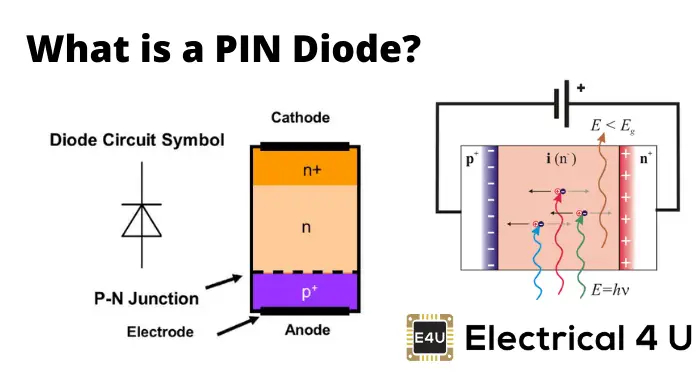
A PIN diode is a type of diode where the intrinsic (I) semiconductor region is sandwiched between the P-type and N-type semiconductor regions, hence the name "PIN." This structure gives it unique properties that make it suitable for various applications, particularly in high-frequency and RF circuits. Here is an overview of PIN diodes:

Structure of a PIN Diode:
-
P-type (P): A region in the diode where the semiconductor material is doped with positively charged holes.
-
Intrinsic (I): The intrinsic or undoped region sits between the P and N layers, making it the key distinguishing feature of a PIN diode. This region is wider than the depletion region in typical diodes.
-
N-type (N): A region where the semiconductor material is doped with negatively charged electrons.
Key Characteristics of PIN Diodes:
-
Low Capacitance: The intrinsic region reduces the capacitance of the diode, making PIN diodes suitable for high-frequency applications where low capacitance is essential.
-
Fast Switching Speed: PIN diodes have fast reverse recovery times, making them ideal for applications requiring quick response times.
-
High Power Handling: Their structure allows PIN diodes to handle high power levels efficiently, making them suitable for power control applications.
-
Variable Resistance: The resistance of a PIN diode varies with the DC bias applied, providing variable attenuation or modulation capabilities.
Applications of PIN Diodes:
-
RF Switches: PIN diodes are commonly used in RF switches to route RF signals due to their fast switching speed and low insertion loss.
-
Attenuators: They are used in adjustable attenuators in RF circuits where variable signal attenuation is required.
-
Phase Shifters: PIN diodes are utilized in phase shifters to electronically control the phase of RF signals.
-
RF Modulators: Their variable resistance characteristics make PIN diodes suitable for use in RF modulators for AM and FM modulation.
-
Photodetectors: In optical communication systems, PIN diodes can function as photodetectors to convert optical signals into electrical signals.
.jpeg)
Working Principle:
-
When a forward bias is applied to the PIN diode, the intrinsic region becomes conductive, allowing current to flow from the P to the N region.
-
In reverse bias, the intrinsic region becomes more resistive, reducing the flow of current through the diode.
Conclusion:
PIN diodes are versatile semiconductor devices with unique characteristics that make them valuable in RF and high-frequency applications where fast switching, low capacitance, and high power handling capabilities are required. Their ability to vary resistance with bias voltage enables their use in various applications ranging from RF switches to attenuators and modulators.


