A semiconductor package is a material that surrounds an integrated circuit or microchip to protect it from physical damage and to provide a medium for electrical connections. It serves as a container for the semiconductor die and facilitates the interconnection between the die and the external environment, typically through leads or pins. The package also helps with heat dissipation and mechanical support.
Here are some key points regarding semiconductor packages:
-
Role of Semiconductor Package:
- Protection: The package shields the delicate semiconductor die from mechanical stress, moisture, contaminants, and other environmental factors that could damage the chip.
- Interconnection: It enables electrical connections between the internal components of the chip and the external system through leads, pins, or solder balls.
- Thermal Management: The package can help dissipate heat generated by the semiconductor device during operation, improving overall performance and reliability.
- Mechanical Support: The package provides structural support for the die and facilitates easy handling during assembly and testing.
-
Types of Semiconductor Packages:
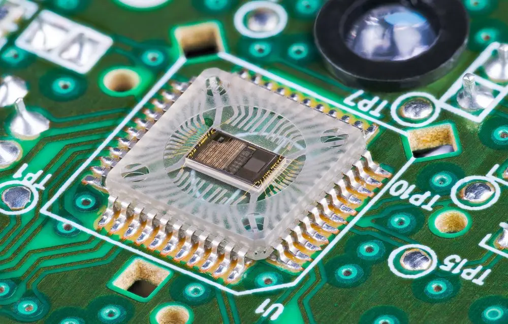
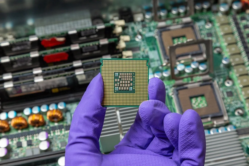
- Dual in-line package (DIP): Traditional through-hole packaging with leads extending from two sides of the package.
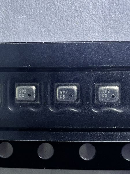
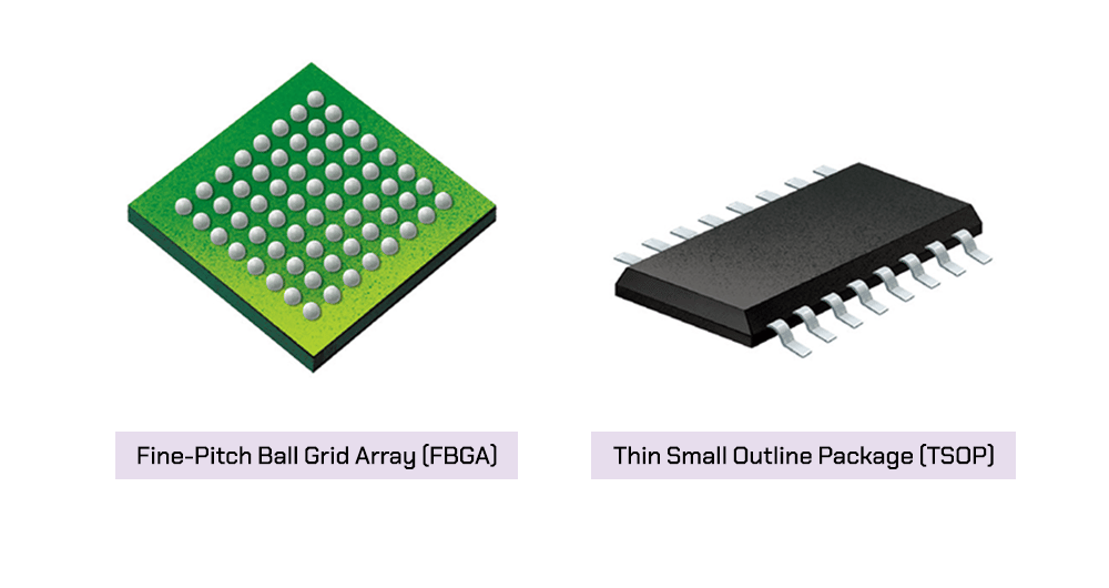
- Surface mount packages (SMD): These include a variety of packages like SOIC, QFP, BGA that sit flush with the surface of the PCB.
- Chip-scale packages (CSP): Extremely compact packages with an area roughly the same size as the die itself.
- Plastic packages: Cost-effective and commonly used packages made from plastic with various configurations.
- Ceramic packages: Provides better thermal performance and reliability, commonly used in high-performance applications.
-
Evolving Trends:
- Semiconductor packaging has evolved to become smaller, denser, and more efficient to meet the demands of high-performance and miniaturized electronic devices.
- Advanced packaging technologies like System-in-Package (SiP), Wafer Level Chip Scale Package (WLCSP), and 3D packaging have emerged to enhance performance and functionality.
-
Considerations:
- When selecting a semiconductor package, factors such as the intended application, cost considerations, thermal requirements, and electrical performance need to be taken into account.
- Different packages offer varying levels of electrical performance, thermal dissipation, and mechanical robustness, so the choice of package can significantly impact the overall performance and reliability of the semiconductor device.
In essence, semiconductor packages are crucial components in the design and production of integrated circuits, providing essential protection, electrical connections, heat dissipation, and mechanical support for semiconductor devices used in a wide range of electronic applications.
Semiconductor package concept explained
A semiconductor package, in the context of integrated circuits (ICs) or semiconductor devices, refers to the housing that encloses the semiconductor die or chip to protect it from physical damage, facilitate electrical connections, aid in thermal management, and provide mechanical support. The package acts as the interface between the internal components of the semiconductor device and the external environment where it is utilized.
Here is a breakdown of the concept of a semiconductor package:
-
Protection: The primary role of a semiconductor package is to shield the sensitive semiconductor die from external factors that could potentially damage it. This includes protection from moisture, dust, mechanical stress, and contamination, ensuring the longevity and reliability of the semiconductor device.
-
Electrical Connections: The semiconductor package provides a means for electrical connections between the internal components of the semiconductor die and the outside world. This is typically achieved through leads, pins, solder balls, or other interconnection mechanisms that allow for signals to be sent to and from the semiconductor device.
-
Thermal Management: Heat dissipation is a critical consideration in semiconductor devices, as excessive heat can degrade performance or even cause the device to fail. The package design may incorporate thermal management features such as heat sinks, thermal vias, or exposed pads to help dissipate heat generated by the semiconductor die during operation.
-
Mechanical Support: The package also offers mechanical support to the semiconductor die, ensuring that it remains securely in place and protected from physical stress or damage. This support is crucial during handling, installation, and operation of the semiconductor device.
-
Varieties of Packages: Semiconductor packages come in a variety of forms, sizes, and materials, each tailored to specific applications and requirements. Common package types include dual in-line packages (DIPs), surface mount packages (SMDs), chip-scale packages (CSPs), plastic packages, and ceramic packages, each offering different attributes in terms of size, cost, thermal performance, and reliability.
-
Evolution in Packaging: Semiconductor packaging technologies have evolved over the years to meet the demands of miniaturization, increased functionality, and improved performance in electronic devices. Advanced packaging techniques such as System-in-Package (SiP), Wafer Level Chip Scale Package (WLCSP), and 3D packaging have emerged to address these requirements.
In summary, a semiconductor package is a crucial component of semiconductor devices, providing essential functions related to protection, electrical connectivity, thermal management, and mechanical support. The choice of package type and design plays a significant role in the overall performance, reliability, and functionality of semiconductor devices in various electronic applications.

Semiconductor package classification
Semiconductor packages are classified based on various factors such as their form factor, mounting method, number of pins, material composition, and intended application. Here are some common classifications based on these factors:
-
By Form Factor:
- Dual in-line package (DIP): Through-hole package with two parallel rows of leads.
- Single in-line package (SIP): Similar to DIP but with a single row of leads.
- Quad flat package (QFP): Square or rectangular package with pins on all four sides.
- Small outline package (SOP/SOIC): Compact and thin package with gull-wing leads.
- Ball grid array (BGA): Package with an array of solder balls on the bottom for surface mounting.
- Chip-scale package (CSP): Ultra-compact package size similar to or slightly larger than the semiconductor die it encapsulates.
-
By Mounting Method:
- Through-Hole Packages: Leads pass through holes in the PCB for soldering.
- Surface Mount Packages (SMD): Components are mounted on the surface of the PCB.
- Flip-Chip Packages: Die is flipped and soldered face-down on the PCB.
- Wire-Bond Packages: Die is connected to the package leads using fine wires.
-
By Pin Count:
- Single Pin Packages: Packages with a single pin or lead, like radial packages.
- Dual Pin Packages: Packages with two pins or leads, like DIP.
- High Pin Count Packages: Packages with a large number of pins, like QFP or BGA.
-
By Material:
- Plastic Packages: Commonly used due to cost-effectiveness and versatility.
- Ceramic Packages: Known for better thermal performance and reliability, typically used in high-end applications.
- Metal Packages: Provide robust mechanical protection and thermal management.
-
By Application:
- Power Packages: Designed for high-power applications, often with additional heat dissipation features.
- Hermetic Packages: Sealed packages to protect sensitive components from environmental factors.
- Optoelectronic Packages: Designed for optical components like LEDs and photodiodes, optimizing light transmission.
-
By Technology:
- Advanced Packaging: Includes technologies like System-in-Package (SiP), Wafer Level Chip Scale Package (WLCSP), and 3D packaging, offering increased functionality and performance.
These classifications help in understanding the diverse range of semiconductor packages available, each tailored to specific requirements in terms of size, performance, thermal characteristics, and assembly techniques in modern electronics manufacturing.